Aug 13, 2026
Minimizing Wafer Micro-Damage: 3 Critical Elastomer Engineering Factors in Automated Handling
In semiconductor fabrication, automated wafer handling systems rely on elastomeric suction cups and edge grips to transfer delicate silicon substrates at high speeds. Because these rubber components directly touch fragile wafer surfaces, any material defect or design flaw can cause yield-killing micro-scratches, stress cracks, electrostatic damage, or particle contamination. Preventing these costly physical defects requires optimizing three essential elastomer engineering factors: advanced non-marking material formulations, stress-distributing contact geometries, and zero-defect automated burr control.
Factor 1: Polymer Formulation for Anti-Static and Low-Outgassing Performance
The foundation of damage-free wafer handling lies in selecting an appropriate polymer matrix. Standard commercial rubber compounds frequently contain volatile plasticizers or sulfur-based curing agents that outgas under vacuum conditions. When brought into contact with silicon substrates, these additives leave microscopic residues that compromise subsequent photolithography or thin-film deposition steps.
Simultaneously, high-speed pick-and-place movements build up static charges that risk electrostatic discharge (ESD) events. Integrating conductive or static-dissipative filler networks directly into the polymer matrix prevents charge accumulation without causing carbon shedding.
Choosing the optimal material requires evaluating thermal limits, outgassing characteristics, ESD protection, and surface hardness. The table below outlines the operational trade-offs among common elastomer families used in substrate contact applications:
| Material Family | Surface Resistivity | Outgassing Level | Micro-Scratch Risk | Primary Application Advantage |
|---|---|---|---|---|
| Conductive Silicone | Low to Moderate | Very Low | Minimal | Excellent flexibility and thermal resistance |
| Fluoroelastomer (FKM) | Ultra-Low | Low | Low | Superior chemical inertness in harsh environments |
| Polyurethane (PU) | Low | Very Low | Minimal | Exceptional abrasion resistance and tear strength |
| ESD-Grade Nitrile (NBR) | Moderate | Low | Moderate | Cost-effective option for non-critical handling |
As shown in the technical matrix, Polyurethane (PU) and ESD-grade silicone deliver low outgassing alongside stable electrostatic dissipation. Selecting materials with a lower elasticity modulus further allows suction pads to deform gently around micro-scale surface variations, distributing clamping force evenly and preventing localized surface marking.
Factor 2: Vacuum Pad Geometry and Stress Distribution
While chemical formulation dictates surface interactions, the physical geometry of the vacuum lip governs force application across the substrate. Conventional suction pads featuring uniform, rigid sealing lips tend to concentrate vacuum pressure into narrow ring-stress zones. Under continuous actuation, these high-stress rings can induce micro-fractures along silicon crystal planes, particularly on thinned wafers.
Optimized pad design uses multi-bellows structures, soft sealing lips, and internal micro-support pillars to spread vacuum suction evenly over a broader area. Furthermore, the lip geometry must balance seal compliance against dynamic stability during rapid robotic moves:
-
Excessive Compliance: Allows the elastomer lip to flex excessively during rapid acceleration, generating friction that sheds micro-particles.
-
Insufficient Compliance: Requires higher vacuum pressure to maintain an airtight seal, increasing localized clamping stress and substrate cracking risks.
By refining contact geometry, vacuum handling systems achieve high holding power at lower differential pressures, protecting delicate substrates from mechanical stress concentration.
Factor 3: Zero-Defect Surface Cleanliness and Burr Control
The final factor focuses on eliminating microscopic manufacturing flash along mold parting lines. In traditional rubber molding, excess material naturally forms small protrusions called burrs or flash. When an elastomer suction pad with microscopic parting-line flash engages a wafer, these rigid protrusions concentrate pressure into micro-point loads.
Under vacuum pressure, unremoved flash causes two failure mechanisms during substrate transfer:
-
Particulate Generation: Micro-burrs shear off due to friction during automated handling, releasing airborne elastomeric particulates directly into cleanroom processing chambers.
-
Localized Substrate Damage: Microscopic flash creates high-pressure point loads capable of scratching protective dielectric films or cracking delicate wafer edges.
Relying on manual post-processing to trim parting-line burrs creates unacceptable quality variations, as human inspection cannot consistently catch sub-millimeter defects in mass production. Achieving reliable surface cleanliness requires fully automated finishing and inspection processes.
Bridging Process Precision and Yield: Next-Generation Elastomer Manufacturing
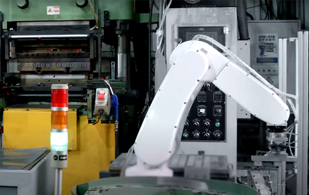
Overcoming these physical contact challenges requires transitioning toward automated, high-precision production environments. Industry leaders such as Sanhao Rubber address burr control issues by deploying automated AI flash inspection equipment alongside 15 collaborative robotic arms. Pairing Japanese six-axis and four-axis SCARA robotics with German injection molding equipment eliminates process variations and contamination risks during pick-and-place, molding, and surface finishing operations.
Additionally, using automated laser cleaning and automated gluing systems allows elastomeric assemblies—including metal-bonded components and custom wafer suction cups—to achieve strong bonding without leaving chemical residues. Backed by data-driven smart manufacturing, modern production facilities deliver 100% automated quality verification, ensuring zero-burr surface cleanliness and tight dimensional stability for advanced substrate handling.
Elevating Substrate Protection through Engineering Excellence
Protecting silicon substrates from micro-damage during automated handling requires addressing physical contact risks at every level. By implementing static-dissipative polymer compounds, stress-distributing vacuum geometries, and automated flash removal, automated production lines can eliminate particle contamination and surface scratching. Adopting precision-molded elastomer components produced under automated quality controls provides a dependable foundation for high-yield semiconductor fabrication.